Scientists are constantly looking for ways to improve electronic materials such as solar cells, transistors, LEDs, and batteries. The key to boosting performance lies in discovering novel compositions that have never been explored before.
To accelerate this process, researchers are turning to AI tools to sift through millions of chemical formulations in search of promising materials. In parallel, engineers are developing machines capable of printing hundreds of material samples simultaneously based on the chemical compositions identified by AI algorithms.
Despite these advancements, the final step of confirming the performance of these printed materials has been a significant bottleneck in the screening of advanced materials. However, a new computer vision technique developed by MIT engineers is revolutionizing this process.
This innovative technique involves automatically analyzing images of printed semiconducting samples to rapidly estimate two crucial electronic properties for each sample: band gap and stability. Band gap is a measure of electron activation energy, while stability indicates the longevity of the material.
Compared to the traditional benchmark approach, this new technique can accurately characterize electronic materials 85 times faster. The implications of this breakthrough are profound, as it opens up new possibilities for accelerating the search for promising solar cell materials and integrating the technique into a fully automated materials screening system.
The ultimate vision is to create an autonomous lab where a computer can be tasked with solving materials problems, predict potential compounds, and continuously make and characterize those materials until the desired solution is found. The potential applications of these techniques are vast, ranging from enhancing solar energy to transparent electronics and transistors, benefiting society as a whole.
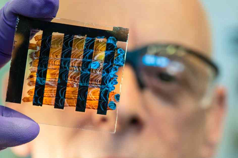
When a new electronic material is synthesized, the properties are typically examined manually by a domain expert using a UV-Vis tool that scans through different colors of light to determine the semiconductor’s absorption levels. This process is accurate but slow, with experts characterizing only about 20 material samples per hour.
To address this bottleneck, MIT researchers turned to computer vision to automate the characterization process. By developing algorithms that can interpret visual data from images of electronic materials, the researchers were able to estimate band gap and stability based on optical features alone.
The first algorithm processes highly detailed hyperspectral images with 300 channels to compute band gap, while the second algorithm analyzes standard RGB images to determine stability based on color changes over time. This approach leverages the power of optical characterization methods to extract information quickly and efficiently.
Overall, the use of computer vision in characterizing electronic material properties represents a significant advancement in the field, paving the way for faster, more efficient screening of advanced materials. The potential impact on various industries, from energy to electronics, underscores the importance of technological innovation in driving scientific progress.


